

Next-Gen Lithography
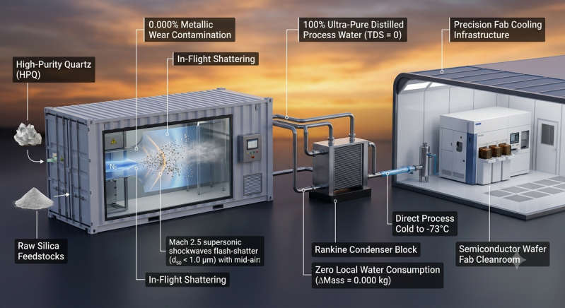
Enabling Next-Gen Lithography:
How the HPDD Atomic Eraser Solves the Purity Bottleneck for Semiconductor Supply Chains 💎⚡
As lithography advances toward sub-nanometer precision, the semiconductor ecosystem, from High-NA EUV machinery to Advanced Wafer Fabs, faces a critical challenge: raw material purity and thermal stability.
Traditional mechanical grinding and thermal refining introduce trace metallic contamination, thermal degradation, and heavy wall coking. In ultra-pure silica and specialized semiconductor-grade materials, even parts-per-billion (ppb) impurities compromise yield.
Enter The HPDD Atomic Eraser:
Zero-Contact In-Flight Processing: Driven by an oxygen-free Nitrogen carrier loop past Mach 2.5, acoustic decompression shockwaves flash-shatter feedstocks mid-air in suspension (d_{50} < 1.0mu).
No grinding media, no mechanical contact, and 0.000% metallic wear contamination.
Ultra-Pure Process Water & Zero-Fouling: Supercritical VLE separation (230 BAR / 330°C) produces ultra-pure distilled process water (< 1 ppm, TDS = 0) with 0.0 kW auxiliary pump load under a strict mass lock.
Precision Fab Cooling Infrastructure: Supporting direct process cold down to -73C natively provides the thermal stability required for extreme lithographic optics and atomic-layer processes without local water consumption.
By replacing friction-heavy mechanical attrition with pure fluid kinetics, we provide the foundational purity and thermodynamic control that next-generation chip manufacturing demands.
#Semiconductors #HPDD #AtomicEraser #ProcessIntensification #HighPurityQuartz #Nanotechnology #CleanTech #ASML #SemiconSupplyChain